The Operational Amplifier
Purpose
To investigate basic operational amplifier circuits.
There are two parts to the lab. In Part (a) we will design a simple 3-bit DAC (Digital to Analog Converter), while in Part (b) we will investigate amplifier gain and clipping.
Part a
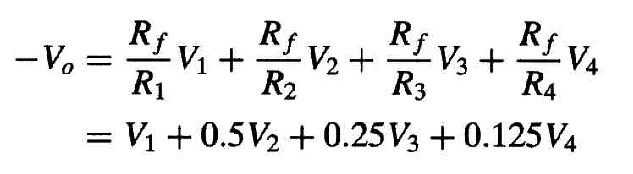
1. The op amp is a fundamental building block in modern instrumentation. It is used extensively in many devices, along with resistors and other passive elements. Its numerous practical applications include digital-to-analog converters, instrumentation amplifiers, level shifters, clippers, calibration circuits, inverters, summers, voltage-to-current converters and current-to-voltage converters, rectifiers, regulators and many more. In this part of the lab we will look at the digital-to-analog converter (DAC). The DAC transforms digital signals (1's and 0's) into analog (voltage level) form. A typical example of a four-bit DAC is illustrated in Block Diagram 1. The four-bit DAC can be realized in many ways. A simple realization is the binary weighted ladder, shown in Circuit 1 which is an inverting summing amplifier. The bits are weighted according to the magnitude of their place value, by descending value of Rf /Rn so that each lesser bit has half the weight of the next higher. The output is related to the inputs as shown below:
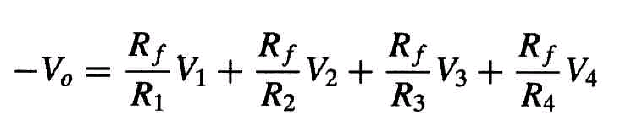
Input V1 is called the most significant bit (MSB), while input V4 is the least significant bit (LSB). Each of the four binary inputs V1...V4 can assume only two voltage levels: 0 or 1 V. By using the proper input and feedback resistor values, the DAC provides a single output that is proportional to the inputs. If we make Rf = 10kW, R1 = 10kW, R2 = 20kW, R3 = 40kW, R4 = 80kW in Circuit 1, then substituting these values in the equation above we get:
The analog output for the binary inputs:
[V1,V2,V3,V4]
= [0000] => -Vo = 0
[V1,V2,V3,V4]
= [0001] => -Vo = 0.125V
[V1,V2,V3,V4]
= [0010] => -Vo = 0.25V
[V1,V2,V3,V4]
= [0011] => -Vo = 0.25V + 0.125V = 0.375V
All 16 combinations of [V1,V2,V3,V4]
and their decimal equivalent along with the voltage output are seen in Table 1.
Design a 3-bit DAC similar to
Circuit 1 such that :
[V1,V2,V3]
= [001] => -Vo = 1.5V ±
0.05V
[V1,V2,V3]
= [010] => -Vo = 3.0V ±
0.05V
[V1,V2,V3]
= [100] => -Vo = 6.0V ±
0.1V
The "-Vo = 1.5V ± 0.05V" indicates that your design can produce 1.45V to 1.55V for an input combination of [001] and be correct. "± 0.05V" is referred to as the design tolerance.
In your design V1,V2 and V3 will be 0V or 1V and make Rf = 6.81kΩ.
We have the following standard resistor values available for your use:
1k, 1.2k, 1.13k, 1.5k 1.8k 2.21k, 2.26k, 2.7k, 3.32k 3.9k, 4,53k, 4.75k 5.62k, 6.81k, 8.25k,
10.0k, 12k, 15.0k, 18k, 22.1k, 27k, 33k, 39k, 47k, 56k, 68k, 82k
2. Draw a circuit diagram for your 3-bit DAC you designed. Look at the datasheet for the Op Amp you are using to get the pin numbers for the inputs, output and power connections. We are using the 8-pin device.
3. Create a table (similar to Table 1) with the 8 combinations of [V1,V2,V3] in ascending order. Here V3 is the least significant digit with a value of 20 or 1, V2 is the next significant digit with a value of 21 or 2 and V1 is the most significant digit with a value of 22 or 4. (It's just like counting in decimal but instead of having ten digits (0...9) there are only two (0,1). Using your standard resistor values chosen above, calculate what you expect -Vo to be for each [V1,V2,V3] combination. Also provide a blank column for the actual values you observe in the lab.
Part b
4. Calculate the gain (V0/Vin) for the inverting amplifier in Circuit 2.
5. You will be testing this circuit with a sinusoidal voltage, which is a voltage that varies sinusoidally with time and we will use the oscilloscope to measure the peak-to-peak amplitude (VPP) of the input and output waveforms Show me how . If a 1VPP sinusoid signal is connected to the input, what will the output level be?
6. With any op amp, the output voltage swing is limited by
the the internal output circuitry and the supply voltage the op amp is operating
at. The datasheet (page 5) states the maximum
Vo is ± 14V with a ±
15V volt supply and a load of 10kW. Knowing you will
be using a ± 15V volt supply and have
the gain calculated above, what is the maximum input signal in volts peak-to
peak (VPP) that can be applied,
before the output "clips" or reaches ±
14V?
Equipment
Proto Board
Op Amp (Fairchild mA741)
DC Power Supply
Short pieces of wire
Resistors (determined by your design)
(resistor color code)
Function Generator
Multimeter
Oscilloscope
Procedure
A. 3-bit DAC
- Using a 741 op-amp, build your 3-bit DAC that you drew the circuit diagram for in Section 2 of the Pre-Lab. Show me how Note you are using the ±15V supply from the Proto Board.
- Connect the Multimeter to the output voltage of the DAC (pin 6).
- Adjust the Hewlett Packard power supply for 1.0V and use it or ground for V1,V2 and V3 when testing your DAC design.
- Go through the table you prepared in Section 3 of the Pre-Lab.
B. Inverting Amplifier
- Change the circuit constructed above so you now have the circuit in Circuit 2. Show me how
- Adjust the Function Generator for a 1kHz sinusoid signal and an output amplitude of 1VPP.
- What is the output voltage? Is it what you calculated in Section 5 of the Pre-Lab.
- Increase the input level until the output starts to "clip" (gets flat on the top and/or bottom of the sign wave). What is the input level? Is it what you expected in Section 6 of the Pre-Lab?
Analysis
1. Discuss the operation of your 3-bit DAC. Were the measured values for -Vo
what was predicted? Were they within the design specification? What was
the cause(s) of any discrepancies?
2. Discuss the operation of the Inverting Amplifier. Was the gain as predicted? Did the op amp "clip" where you expected it to? Was the datasheet correct?